From “Made in” to “Designed by” Malaysia - The IC Design Park’s Strategic Shift
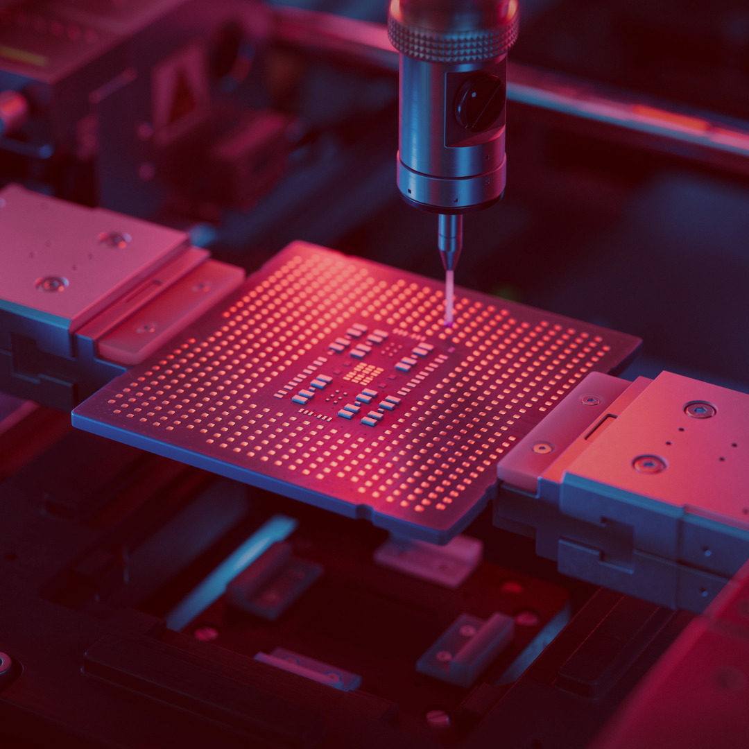
Malaysia already plays a crucial role in global semiconductors, handling 13% of the world’s chip testing and packaging (Reuters). Now, the country is moving up the value chain into IC design, a high-value segment that shapes the performance, efficiency, and competitiveness of chips before they even reach the manufacturing line.
The IC Design Park Vision
Launched in August 2024, the Malaysia Semiconductor IC Design Park in Puchong represents a partnership between state and federal governments, industry leaders, and global technology firms. The facility aims to provide:
• Design Infrastructure – State-of-the-art CAD tools, prototyping labs, and simulation environments.
• Talent Development – Partnerships with universities to produce industry-ready chip designers.
• Commercial Acceleration – Support for start-ups and SMEs to bring new chip designs to market.
Economic Impact
The ARM partnership alone is expected to:
• Produce 7 high-end chip blueprints for Malaysian companies.
• Train 10,000 engineers in advanced chip design methodologies.
• Enable local firms to compete for contracts currently dominated by U.S., Taiwanese, and South Korean giants.
Combined with Malaysia’s $107 billion investment ambition, this move positions the nation to capture a larger share of the semiconductor value chain, which was worth $574 billion globally in 2022 and is projected to hit $1 trillion by 2030 (McKinsey).
Why It Matters
Moving from “Made in Malaysia” to “Designed by Malaysia” not only increases value capture but also builds IP ownership, strengthens national security in tech, and creates higher-paying, knowledge-based jobs.
Learn more about Malaysia’s semiconductor transformation at the Selangor Techsphere Summit 2025.